FIRST ORDER
FREE 10% DISCOUNT




Microsemi Corporation
Alarms, Buzzers, and Sirens
-
Stacked
Scrolling
|
Img
|
Pdf
|
Part Number
|
Manufacturers
|
Desc
|
In Stock
|
Packing
|
Rfq
|
||||||||||||||||||||||
|---|---|---|---|---|---|---|---|---|---|---|---|---|---|---|---|---|---|---|---|---|---|---|---|---|---|---|---|---|---|
|
|

|
Linear Voltage Regulator IC Positive Fixed 1 Output 4.6A TO-263, Power
|
3458
|
TO-263-4, D²Pak (3 Leads + Tab), TO-263AA
|
|
||||||||||||||||||||||||
|
|
Zener Diode 160 V 2 W ±5% Surface Mount SMBG (DO-215AA)
|
8620
|
DO-215AA, SMB Gull Wing
|
|
||||||||||||||||||||||||
|
|
|
LED Driver IC 32 Output Shift Register PWM Dimming 200mA 56-QFN (8x8)
|
4615
|
56-VFQFN Exposed Pad
|
|
||||||||||||||||||||||||
|
|
|
Linear Voltage Regulator IC Positive Fixed 1 Output 3A TO-263, Power
|
4225
|
TO-263-4, D²Pak (3 Leads + Tab), TO-263AA
|
|
||||||||||||||||||||||||
|
|
|
Zener Diode 3.6 V 2 W ±2% Surface Mount SMBJ (DO-214AA)
|
2479
|
DO-214AA, SMB
|
|
||||||||||||||||||||||||
|
|
|
Power Switch/Driver 1:1 P-Channel 2.8A 20-CSOIC, Flat Leads
|
8161
|
20-CFlatPack
|
|
||||||||||||||||||||||||
|
|
|
Supervisor Open Drain or Open Collector 1 Channel 8-SOIC
|
1518
|
8-SOIC (0.154", 3.90mm Width)
|
|
||||||||||||||||||||||||
|
|
|
Zener Diode 7.5 V 2 W ±2% Surface Mount SMBJ (DO-214AA)
|
8558
|
DO-214AA, SMB
|
|
||||||||||||||||||||||||
|
|
|
Bipolar (BJT) Transistor NPN 800 V 1 A 4 W Through Hole TO-5
|
7000
|
TO-205AA, TO-5-3 Metal Can
|
|
||||||||||||||||||||||||
|
|
|
Shunt Voltage Reference IC Adjustable 2.5V 36 VV ±1% 100 mA 8-SOIC
|
5346
|
8-SOIC (0.154", 3.90mm Width)
|
|
||||||||||||||||||||||||
|
|
|
Zener Diode 16 V 2 W ±2% Surface Mount SMBJ (DO-214AA)
|
6247
|
DO-214AA, SMB
|
|
||||||||||||||||||||||||
|
|
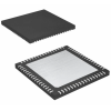
IGLOO nano Field Programmable Gate Array (FPGA) IC 49 768 68-VFQFN Exposed Pad General Description The IGLOO family of flash FPGAs, based on a 130-nm flash process, offers the lowest power FPGA, a single-chip solution, small footprint packages, reprogrammability, and an abundance of advanced features. The Flash*Freeze technology used in IGLOO nano devices enables entering and exiting an ultra-low power mode that consumes nanoPower while retaining SRAM and register data. Flash*Freeze technology simplifies power management through l/O and clock management with rapid recovery to operation mode. The Low Power Active capability (static idle) allows for ultra-low power consumption while the IGLOO nano device is completely functional in the system. This allows the IGLO0 nano device to control system power management based on external inputs (e.g., scanning for keyboard stimulus) while consuming minimal power. Nonvolatile flash technology gives lGLOO nano devices the advantage of being a secure, low power, single-chip solution that is Instant On. The IGLOO nano device is reprogrammable and offers time-to-market benefits at an ASIC-level unit cost. These features enable designers to create high-density systems using existing ASIC or FPGA design flows and tools. IGLOO nano devices offer 1 kbit of on-chip, reprogrammable, nonvolatile FlashROM storage as well as clock conditioning circuitry based on an integrated phase-locked loop (PLL). The AGLN030 and smaller devices have no PLL or RAM support. IGLOO nano devices have up to 250 k system gates, supported with up to 36 kbits of true dual-port SRAM and up to 71 user l/Os. IGLOO nano devices increase the breadth of the IGLOO product line by adding new features and packages for greater customer value in high volume consumer, portable, and battery-backed markets. Features such as smaller footprint packages designed with two-layer PCBs in mind, power consumption measured in nanoPower, Schmitt trigger, and bus hold (hold previous l/O state in Flash*Freeze mode) functionality make these devices ideal for deployment in applications that require high levels of flexibility and low cost. Features and Benefits
nanoPower Consumption-Industry's Lowest Power 1.2 V to 1.5 V Core Voltage Support for Low Power Supports Single-Voltage System Operation Low Power Active FPGA Operation Flash*Freeze Technology Enables Ultra-Low Power Consumption while MaintainingFPGA Content Easy Entry to / Exit from Ultra-Low Power Flash*Freeze Mode
As Small as 3x3 mm in Size
10,000 to 250,000 System Gates Up to 36 kbits of True Dual-Port SRAM Up to 71 User 1/Os
130-nm, 7-Layer Metal, Flash-Based CMOS Process Instant On Level 0 Support Single-Chip Solution Retains Programmed Design When Powered Off 250 MHz (1.5 V systems) and 160 MHz (1.2 V systems) System Performance
ISP Using On-Chip 128-BitAdvanced Encryption Standard (AES) Decryption via JTAG (IEEE 1532-compliant) FlashLock®Designed to Secure FPGA Contents 1.2 V Programming
Segmented,Hierarchical Routing and Clock Structure
1.2 V, 1.5 V, 1.8 V, 2.5 V,and 3.3 V Mixed-Voltage Operation Bank-Selectable I/O Voltages-up to 4 Banks per Chip Single-Ended I/O Standards:LVTTL,LVCMOS 3.3V/2.5 V/ 1.8 V/1.5 V/1.2V Wide Range Power Supply Voltage Support per JESD8-B, Allowing I/Os to Operate from 2.7 V to 3.6V Wide Range Power Supply Voltage Support per JESD8-12, Allowing I/Os to Operate from 1.14 V to 1.575V I/O Registers on Input, Output, and Enable Paths Selectable Schmitt Trigger Inputs Hot-Swappable and Cold-Sparing I/Os Programmable Output Slew Rate and Drive Strength Weak Pull-Up/-Down IEEE 1149.1(JTAG) Boundary Scan Test Pin-Compatible Packages across the IGLOO®Family
Up to Six CCC Blocks, One with an Integrated PLL Configurable Phase Shift, Multiply/Divide, Delay Capabilities, and External Feedback Wide Input Frequency Range (1.5 MHz up to 250 MHz)
1 kbit of FlashROM User Nonvolatile Memory SRAMs and FIFOs with Variable-Aspect-Ratio4,608-Bit RAM Blocks (x1, x2, x4, x9, and x18 organizations) True Dual-Port SRAM(except x18 organization)
Tj=-20℃ to +85℃ How to choose FPGA for your project?
|
3726
|
68-VFQFN Exposed Pad
|
|
||||||||||||||||||||||||
|
|
|
Boost, Buck, Flyback, Forward Regulator Positive, Isolation Capable Output Step-Up, Step-Down DC-DC Controller IC 14-SOIC
|
8756
|
14-SOIC (0.154", 3.90mm Width)
|
|
||||||||||||||||||||||||
|
|
|
Zener Diode 36 V 2 W ±2% Surface Mount SMBJ (DO-214AA)
|
2098
|
DO-214AA, SMB
|
|
||||||||||||||||||||||||
|
|
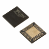
IGLOO Field Programmable Gate Array (FPGA) IC 84 36864 3072 132-WFQFN General Description The IGLOO family of flash FPGAs, based on a 130-nm flash process, offers the lowest power FPGA, a single-chip solution, small footprint packages, reprogrammability, and an abundance of advanced features. The Flash*Freeze technology used in IGLOO devices enables entering and exiting an ultra-low power mode that consumes as little as 5 μW while retaining SRAM and register data. Flash*Freeze technology simplifies power management through I/O and clock management with rapid recovery to operation mode. The Low Power Active capability (static idle) allows for ultra-low power consumption (from 12 μW) while the IGLOO device is completely functional in the system. This allows the IGLOO device to control system power management based on external inputs (e.g., scanning for keyboard stimulus) while consuming minimal power. Nonvolatile flash technology gives IGLOO devices the advantage of being a secure, low power, single-chip solution that is Instant On. IGLOO is reprogrammable and offers time-to-market benefits at an ASIC-level unit cost. These features enable designers to create high-density systems using existing ASIC or FPGA design flows and tools. IGLOO devices offer 1 kbit of on-chip, reprogrammable, nonvolatile FlashROM storage as well as clock conditioning circuitry based on an integrated phase-locked loop (PLL). The AGL015 and AGL030 devices have no PLL or RAM support. IGLOO devices have up to 1 million system gates, supported with up to 144 kbits of true dual-port SRAM and up to 300 user I/Os. M1 IGLOO devices support the high-performance, 32-bit Cortex-M1 processor developed by ARM for implementation in FPGAs. Cortex-M1 is a soft processor that is fully implemented in the FPGA fabric. It has a three-stage pipeline that offers a good balance between low power consumption and speed when implemented in an M1 IGLOO device. The processor runs the ARMv6-M instruction set, has a configurable nested interrupt controller, and can be implemented with or without the debug block. Cortex-M1 is available for free from Microsemi for use in M1 IGLOO FPGAs. The ARM-enabled devices have ordering numbers that begin with M1AGL and do not support AES decryption. Features and Benefits
1.2 V to 1.5 V Core Voltage Support for Low Power Supports Single-Voltage System Operation 5 μW Power Consumption in Flash*Freeze Mode Low Power Active FPGA Operation Flash*Freeze Technology Enables Ultra-Low Power Consumption while MaintainingFPGA Content Easy Entry to / Exit from Ultra-Low Power Flash*Freeze Mode
15K to 1 Million System Gates Up to 144 Kbits of True Dual-Port SRAM Up to 300 User 1/Os
130-nm, 7-Layer Metal, Flash-Based CMOS Process Instant On Level 0 Support Single-Chip Solution Retains Programmed Design When Powered Off 250 MHz (1.5 V systems) and 160 MHz (1.2 V systems) System Performance
ISP Using On-Chip 128-Bit Advanced Encryption Standard (AES) Decryption (except ARM®-enabled IGLOO®devices) via JTAG (IEEE 1532-compliant) FlashLock®Designed to Secure FPGA Contents
Segmented, Hierarchical Routing and Clock Structure
700 Mbps DDR,LVDS-Capable I/Os (AGL250 and above) 1.2 V, 1.5 V, 1.8 V, 2.5V, and 3.3 V Mixed-Voltage Operation Bank-Selectable I/O Voltages--up to 4 Banks per Chip Single-Ended I/O Standards:LVTTL,LVCMOS 3.3V/2.5 V/ 1.8 V /1.5 V/ 1.2 .V, 3.3 V PCI/ 3.3 V PCI-X, and LVCMOS 2.5 V/5.0V Input DifferentialI/O Standards:LVPECL,LVDS,B-LVDS,and M-LVDS (AGL250 and above) Wide Range Power Supply Voltage Support per JESD8-B, Allowing I/Os to Operate from 2.7 V to 3.6 V Wide Range Power Supply Voltage Support per JESD8-12, Allowing I/Os to Operate from 1.14 V to 1.575V I/O Registers on Input, Output, and Enable Paths Hot-Swappable and Cold-Sparing,I/Os+ Programmable Output Slew Rateand Drive Strength Weak Pull-Up/-Down IEEE 1149.1 (JTAG) Boundary Scan Test Pin-Compatible Packages across the IGLOO Family
Six CCC Blocks, One with an Integrated PLL Configurable Phase Shift, Multiply/Divide,Delay Capabilities, and External Feedback Wide Input Frequency Range (1.5 MHz up to 250 MHz)
1 kbit of FlashROM User Nonvolatile Memory SRAMs and FIFOs with Variable-Aspect-Ratio4,608-Bit RAM Blocks (x1,x2,x4, x9, and x18 organizations) True Dual-Port SRAM (except x18)
M1 IGLOO Devices--Cortex®-M1 Soft Processor Available with or without Debug How to choose FPGA for your project?
|
1969
|
132-WFQFN
|
|
||||||||||||||||||||||||
|
|
|
Zener Diode 5.6 V 3 W ±5% Through Hole DO-204AL (DO-41)
|
3412
|
DO-204AL, DO-41, Axial
|
|
||||||||||||||||||||||||
|
|
|
Zener Diode 75 V 2 W ±2% Surface Mount SMBJ (DO-214AA)
|
8300
|
DO-214AA, SMB
|
|
||||||||||||||||||||||||
|
|
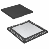
ProASIC3 Field Programmable Gate Array (FPGA) IC 49 68-VFQFN Exposed Pad General Description ProASIC3,the third-generation family of Microsemi flash FPGAs, offers performance, density, and features beyond those of the ProASICPLUS® family. Nonvolatile flash technology gives ProASIC3 devices the advantage of being a secure, low power, single-chip solution that is Instant On. ProASIC3 is reprogrammable and offers time-to-market benefits at an ASIC-level unit cost. These features enable designers to create high-density systems using existing ASIC or FPGA design flows and tools. ProASIC3 devices offer 1 kbit of on-chip, reprogrammable, nonvolatile FlashROM storage as well as clock conditioning circuitry based on an integrated phase-locked loop (PLL). The A3P015 and A3P030 devices have no PLL or RAM support. ProASIC3 devices have up to 1 million system gates, supported with up to 144 kbits of true dual-port SRAM and up to 300 user I/Os. ProASIC3 devices support the ARM Cortex-M1 processor. The ARM-enabled devices have Microsemi ordering numbers that begin with M1A3P (Cortex-M1) and do not support AES decryption. Features and Benefits
15 K to 1 M System Gates Up to 144 Kbits of True Dual-Port SRAM Up to 300 User I/Os
130-nm, 7-Layer Metal (6 Copper), Flash-Based CMOS Process Instant On Level 0 Support Single-Chip Solution Retains Programmed Design when Powered Off
350 MHz System Performance 3.3 V, 66 MHz 64-Bit PCI
ISP Using On-Chip 128-Bit Advanced Encryption Standard (AES) Decryption (except ARM®-enabled ProASIC®3 devices) via JTAG (IEEE 1532-compliant) FlashLock® to Secure FPGA Contents
Core Voltage for Low Power Support for 1.5V-Only Systems Low-Impedance Flash Switches
Segmented, Hierarchical Routing and Clock Structure
700 Mbps DDR,LVDS-Capable I/Os (A3P250 and above) 1.5V, 1.8 V, 2.5 V,and 3.3V Mixed-Voltage Operation Wide Range Power Supply Voltage Support per JESD8-B, Allowing I/Os to Operate from 2.7 V to 3.6 V Bank-Selectable I/O Voltages—up to 4 Banks per Chip Single-Ended I/O Standards: LVTTL, LVCMOS 3.3V / 2.5V / 1.8V / 1.5V, 3.3V PCI / 3.3V PCI-X and LVCMOS 2.5V / 5.0V Input Differential I/O Standards: LVPECL,LVDS,B-LVDS, and M-LVDS (A3P250 and above) I/O Registers on Input, Output, and Enable Paths Hot-Swappable and Cold Sparing I/Os Programmable Output Slew Rate and Drive Strength Weak Pull-Up/-Down IEEE 1149.1 (JTAG) Boundary Scan Test Pin-Compatible Packages across the ProASIC3 Family
Six CCC Blocks, One with an Integrated PLL Configurable Phase-Shift, Multiply/Divide, Delay Capabilities and External Feedback Wide Input Frequency Range (1.5 MHz to 350 MHz)
1 Kbit of FlashROM User Nonvolatile Memory SRAMs and FIFOs with Variable-Aspect-Ratio 4,608-Bit RAM Blocks (x1, x2, x4, x9, and x18 organizations) True Dual-Port SRAM (except x18)
M1 ProASIC3 Devices-ARM®Cortex®-M1 Soft Processor Available with or without Debug |
5355
|
68-VFQFN Exposed Pad
|
|
||||||||||||||||||||||||
|
|
|
N-Channel 100 V 100A (Tc) 625W (Tc) Through Hole T-MAX™ [B2]
|
4603
|
TO-247-3 Variant
|
|
||||||||||||||||||||||||
|
|
|
Zener Diode 3.9 V 5 W ±10% Surface Mount SMBJ (DO-214AA)
|
3836
|
DO-214AA, SMB
|
|
||||||||||||||||||||||||
|
|
ProASIC3L Field Programmable Gate Array (FPGA) IC 151 36864 208-BFQFP Clock Frequency Synthesis Deriving clocks of various frequencies from a single reference clock is known as frequency synthesis.The PLL has an input frequency range from 1.5 to 350 MHz. This frequency is automatically divideddown to a range between 1.5 MHz and 5.5 MHz by input dividers (not shown in Figure 4-19 on page 100)between PLL macro inputs and PLL phase detector inputs. The VCO output is capable of an outputrange from 24 to 350 MHz. With dividers before the input to the PLL core and following the VCO outputs,the VCO output frequency can be divided to provide the final frequency range from 0.75 to 350 MHz.Using SmartGen, the dividers are automatically set to achieve the closest possible matches to thespecified output frequencies. Users should be cautious when selecting the desired PLL input and output frequencies and the I/O bufferstandard used to connect to the PLL input and output clocks. Depending on the I/O standards used forthe PLL input and output clocks, the I/O frequencies have different maximum limits. Refer to the familydatasheets for specifications of maximum I/O frequencies for supported I/O standards. Desired PLL inputor output frequencies will not be achieved if the selected frequencies are higher than the maximum I/Ofrequencies allowed by the selected I/O standards. Users should be careful when selecting the I/Ostandards used for PLL input and output clocks. Performing post-layout simulation can help detect thistype of error, which will be identified with pulse width violation errors. Users are strongly encouraged toperform post-layout simulation to ensure the I/O standard used can provide the desired PLL input oroutput frequencies. Users can also choose to cascade PLLs together to achieve the high frequenciesneeded for their applications. Details of cascading PLLs are discussed in the "Cascading CCCs" sectionon page 125. In SmartGen, the actual generated frequency (under typical operating conditions) will be displayedbeside the requested output frequency value. This provides the ability to determine the exact frequencythat can be generated by SmartGen, in real time. The log file generated by SmartGen is a useful tool indetermining how closely the requested clock frequencies match the user specifications. For example,assume a user specifies 101 MHz as one of the secondary output frequencies. If the best outputfrequency that could be achieved were 100 MHz, the log file generated by SmartGen would indicate theactual generated frequency How to choose FPGA for your project?
|
7139
|
208-BFQFP
|
|
||||||||||||||||||||||||
|
|
|
IGBT PT 600 V 56 A 250 W Through Hole TO-220 [K]
|
3763
|
TO-220-3
|
|
||||||||||||||||||||||||
|
|
|
Zener Diode 5.1 V 5 W ±10% Surface Mount SMBJ (DO-214AA)
|
6288
|
DO-214AA, SMB
|
|
||||||||||||||||||||||||
|
|
Fusion® Field Programmable Gate Array (FPGA) IC 37 27648 108-WFQFN General Description The Fusion family, based on the highly successful ProASIC®3 and ProASIC3E flash FPGA architecture,has been designed as a high-performance, programmable, mixed signal platform. By combining anadvanced flash FPGA core with flash memory blocks and analog peripherals, Fusion devicesdramatically simplify system design and, as a result, dramatically reduce overall system cost and boardspace. The state-of-the-art flash memory technology offers high-density integrated flash memory blocks,enabling savings in cost, power, and board area relative to external flash solutions, while providingincreased flexibility and performance. The flash memory blocks and integrated analog peripherals enabletrue mixed-mode programmable logic designs. Two examples are using an on-chip soft processor toimplement a fully functional flash MCU and using high-speed FPGA logic to offer system and powersupervisory capabilities. Instant On, and capable of operating from a single 3.3 V supply, the Fusionfamily is ideally suited for system management and control applications. The devices in the Fusion family are categorized by FPGA core density. Each family member containsmany peripherals, including flash memory blocks, an analog-to-digital-converter (ADC), high-driveoutputs, both RC and crystal oscillators, and a real-time counter (RTC). This provides the user with ahigh level of flexibility and integration to support a wide variety of mixed signal applications. The flashmemory block capacity ranges from 2 Mbits to 8 Mbits. The integrated 12-bit ADC supports up to 30independently configurable input channels. The on-chip crystal and RC oscillators work in conjunction with the integrated phase-locked loops (PLLs)to provide clocking support to the FPGA array and on-chip resources. In addition to supporting typicalRTC uses such as watchdog timer, the Fusion RTC can control the on-chip voltage regulator to powerdown the device (FPGA fabric, flash memory block, and ADC), enabling a low power standby mode. The Fusion family offers revolutionary features, never before available in an FPGA. The nonvolatile flashtechnology gives the Fusion solution the advantage of being a highly secure, low power, single-chipsolution that is Instant On. Fusion is reprogrammable and offers time-to-market benefits at an ASIC-levelunit cost. These features enable designers to create high-density systems using existing ASIC or FPGAdesign flows and tools. Features and Benefits
Advanced 130-nm, 7-Layer Metal, Flash-Based CMOSProcess Nonvolatile, Retains Program when Powered Off Instant On Single-Chip Solution 350 MHz System Performance
User Flash Memory–2 Mbits to 8 Mbits – Configurable 8-, 16-, or 32-Bit Datapath – 10 ns Access in Read-Ahead Mode 1 Kbit of Additional FlashROM
Up to 12-Bit Resolution and up to 600 Ksps Internal 2.56 V or External Reference Voltage ADC: Up to 30 Scalable Analog Input Channels High-Voltage Input Tolerance: –10.5 V to +12 V Current Monitor and Temperature Monitor Blocks Up to 10 MOSFET Gate Driver Outputs – P- and N-Channel Power MOSFET Support – Programmable 1, 3, 10, 30 µA, and 20 mA DriveStrengths ADC Accuracy is Better than 1%
Internal 100 MHz RC Oscillator (accurate to 1%) Crystal Oscillator Support (32 KHz to 20 MHz) Programmable Real-Time Counter (RTC) 6 Clock Conditioning Circuits (CCCs) with 1 or 2 Integrated PLLs – Phase Shift, Multiply/Divide, and Delay Capabilities – Frequency: Input 1.5–350 MHz, Output 0.75–350 MHz
Single 3.3 V Power Supply with On-Chip 1.5 V Regulator Sleep and Standby Low-Power Modes
ISP with 128-Bit AES via JTAG FlashLock® Designed to Protect FPGA Contents
1.5 V, 1.8 V, 2.5 V, and 3.3 V Mixed-Voltage Operation Bank-Selectable I/O Voltages – Up to 5 Banks per Chip Single-Ended I/O Standards: LVTTL, LVCMOS 3.3V/2.5V/1.8V/1.5V,3.3V PCI/3.3V PCI-X, and LVCMOS 2.5V/5.0 V Input Differential I/O Standards: LVPECL, LVDS, B-LVDS,M-LVDS – Built-In I/O Registers – 700 Mbps DDR Operation Hot-Swappable I/Os Programmable Output Slew Rate, Drive Strength, and Weak Pull-Up/Down Resistor Pin-Compatible Packages across the Fusion® FamilySRAMs and FIFOs Variable-Aspect-Ratio 4,608-Bit SRAM Blocks (×1, ×2,×4, ×9, and ×18 organizations available) True Dual-Port SRAM (except ×18) Programmable Embedded FIFO Control Logic
ARM® Cortex-™M1–Enabled
Targeted to Pigeon Point® Board ManagementReference (BMR) Starter Kits Designed in Partnership with Pigeon Point Systems ARM Cortex-M1 Enabled
Targeted to Advanced Mezzanine Card (AdvancedMC™Designs) Designed in Partnership with MicroBlade 8051-Based Module Management Controller (MMC) How to choose FPGA for your project?
|
1483
|
108-WFQFN
|
|
||||||||||||||||||||||||
|
|
|
N-Channel 200 V 100A (Tc) 520W (Tc) Through Hole T-MAX™ [B2]
|
4119
|
TO-247-3 Variant
|
|
||||||||||||||||||||||||
|
|
|
Zener Diode 100 V 5 W ±10% Surface Mount SMBJ (DO-214AA)
|
9102
|
DO-214AA, SMB
|
|
||||||||||||||||||||||||
|
|
|
Diode 200 V 45A Surface Mount D3 [S]
|
2712
|
TO-268-3, D³Pak (2 Leads + Tab), TO-268AA
|
|
||||||||||||||||||||||||
|
|
|
Zener Diode 150 V 5 W ±2% Surface Mount SMBJ (DO-214AA)
|
6367
|
DO-214AA, SMB
|
|
||||||||||||||||||||||||
|
|
|
N-Channel 1000 V 5A (Tc) 225W (Tc) Through Hole TO-220 [K]
|
3436
|
TO-220-3
|
|
||||||||||||||||||||||||
|
|
|
Zener Diode 4.7 V 2 W ±5% Surface Mount SMBJ (DO-214AA)
|
5150
|
DO-214AA, SMB
|
|
||||||||||||||||||||||||