FIRST ORDER
FREE 10% DISCOUNT


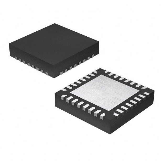
A Comprehensive Guide To LCMXO2-1200HC-6SG32C MachXO2 Field Programmable Gate Array (FPGA) IC 21 65536 1280 32-UFQFN Exposed Pad
- Manufacturer: Lattice Semiconductor Corporation
- Product NO: LCMXO2-1200HC-6SG32C
- Package: 32-UFQFN Exposed Pad
- Datasheet:
 PDF
PDF - Stock: 4240
- Sample Price: $7.7
- Bulk purchase price:
- Description: MachXO2 Field Programmable Gate Array (FPGA) IC 21 65536 1280 32-UFQFN Exposed PadGeneral DescriptionThe MachXO2 family Notice:
Unconfirmed payment orders may not be able to deliver the normal cancellation of the order, please communicate with the email to confirm before making the relevant payment ~ Attached email phone number The platform has the right to cancel the unconfirmed payment orders do not need to bear the responsibility of default.
Payment and disbursement


| Parameters |
|---|
MachXO2 Field Programmable Gate Array (FPGA) IC 21 65536 1280 32-UFQFN Exposed Pad
General Description
The MachXO2 family of ultra low power, instant-on, non-volatile PLDs has six devices with densities ranging from 256 to
6864 Look-Up Tables (LUTs). In addition to LUT-based, low-cost programmable logic these devices feature Embedded
Block RAM (EBR), Distributed RAM, User Flash Memory (UFM), Phase Locked Loops (PLLs), preengineered source
synchronous I/O support, advanced configuration support including dual-boot capability and hardened versions of
commonly used functions such as SPI controller, I²C controller and timer/counter. These features allow these devices to
be used in low cost, high volume consumer and system applications.
The MachXO2 devices are designed on a 65 nm non-volatile low power process. The device architecture has several
features such as programmable low swing differential I/Os and the ability to turn off I/O banks, on-chip PLLs and
oscillators dynamically. These features help manage static and dynamic power consumption resulting in low static power
for all members of the family.
The MachXO2 devices are available in two versions – ultra low power (ZE) and high performance (HC and HE) devices.
The ultra low power devices are offered in three speed grades –1, –2 and –3, with –3 being the fastest. Similarly, the
high-performance devices are offered in three speed grades: –4, –5 and –6, with –6 being the fastest. HC devices have an
internal linear voltage regulator which supports external VCC supply voltages of 3.3 V or 2.5 V. ZE and HE devices only
accept 1.2 V as the external VCC supply voltage. With the exception of power supply voltage all three types of devices
(ZE, HC and HE) are functionally compatible and pin compatible with each other.
The MachXO2 PLDs are available in a broad range of advanced halogen-free packages ranging from the space saving
2.5 mm x 2.5 mm WLCSP to the 23 mm x 23 mm fpBGA. MachXO2 devices support density migration within the same
package. Table 1-1 shows the LUT densities, package and I/O options, along with other key parameters.
The pre-engineered source synchronous logic implemented in the MachXO2 device family supports a broad range of
interface standards, including LPDDR, DDR, DDR2 and 7:1 gearing for display I/Os.
The MachXO2 devices offer enhanced I/O features such as drive strength control, slew rate control, PCI compati bility,
bus-keeper latches, pull-up resistors, pull-down resistors, open drain outputs and hot socketing. Pull-up, pull-down and
bus-keeper features are controllable on a“per-pin”basis.
A user-programmable internal oscillator is included in MachXO2 devices. The clock output from this oscillator may be
divided by the timer/counter for use as clock input in functions such as LED control, key-board scanner and sim-ilar state
machines.
The MachXO2 devices also provide flexible, reliable and secure configuration from on-chip Flash memory. These devices
can also configure themselves from external SPI Flash or be configured by an external master through the JTAG test
access port or through the I2C port. Additionally, MachXO2 devices support dual-boot capability (using external Flash
memory) and remote field upgrade (TransFR) capability.
Lattice provides a variety of design tools that allow complex designs to be efficiently implemented using the MachXO2
family of devices. Popular logic synthesis tools provide synthesis library support for MachXO2. Lattice design tools use the
synthesis tool output along with the user-specified preferences and constraints to place and route the design in the
MachXO2 device. These tools extract the timing from the routing and back-annotate it intothe design for timing
verification.
Lattice provides many pre-engineered IP (Intellectual Property) LatticeCORE™ modules, including a number of reference
designs licensed free of charge, optimized for the MachXO2 PLD family. By using these configurable soft core IP cores as
standardized blocks, users are free to concentrate on the unique aspects of their design, increasing their productivity.
Features
Flexible Logic Architecture
Six devices with 256 to 6864 LUT4s and 18 to 334 I/Os
Ultra Low Power Devices
Advanced 65 nm low power process
As low as 22 µW standby power
Programmable low swing differential I/Os
Stand-by mode and other power saving options
Embedded and Distributed Memory
Up to 240 kbits sysMEM™ Embedded BlockRAM
Up to 54 kbits Distributed RAM
Dedicated FIFO control logic
On-Chip User Flash Memory
Up to 256 kbits of User Flash Memory
100,000 write cycles
Accessible through WISHBONE, SPI, I2C and JTAG interfaces
Can be used as soft processor PROM or as Flash memory
Pre-Engineered Source Synchronous I/O
DDR registers in I/O cells
Dedicated gearing logic
7:1 Gearing for Display I/Os
Generic DDR, DDRX2, DDRX4
Dedicated DDR/DDR2/LPDDR memory with DQS support
High Performance, Flexible I/O Buffer
Programmable sysIO™ buffer supports wide range of interfaces:
– LVCMOS 3.3/2.5/1.8/1.5/1.2
– LVTTL
– PCI
– LVDS, Bus-LVDS, MLVDS, RSDS, LVPECL
– SSTL 25/18
– HSTL 18
– Schmitt trigger inputs, up to 0.5 V hysteresis
I/Os support hot socketing
On-chip differential termination
Programmable pull-up or pull-down mode
Flexible On-Chip Clocking
Eight primary clocks
Up to two edge clocks for high-speed I/O interfaces (top and bottom sides only)
Up to two analog PLLs per device with fractional-n frequency synthesis
– Wide input frequency range (7 MHz to 400 MHz)
Non-volatile, Infinitely Reconfigurable
Instant-on – powers up in microseconds
Single-chip, secure solution
Programmable through JTAG, SPI or I²C
Supports background programming of non-vola-tile memory
Optional dual boot with external SPI memory
TransFR™ Reconfiguration
In-field logic update while system operates
Enhanced System Level Support
On-chip hardened functions: SPI, I²C, timer/counter
On-chip oscillator with 5.5% accuracy
Unique TraceID for system tracking
One Time Programmable (OTP) mode
Single power supply with extended operating range
IEEE Standard 1149.1 boundary scan
IEEE 1532 compliant in-system programming
Broad Range of Package Options
TQFP, WLCSP, ucBGA, csBGA, caBGA, ftBGA, fpBGA, QFN package options
Small footprint package options
– As small as 2.5 mm x 2.5 mm
Density migration supported
Advanced halogen-free packaging
How to choose FPGA for your project?
Hot Sales
S9KEAZ128AMLH
ARM® Cortex®-M0+ Kinetis KEA Microcontroller IC 32-Bit Single-Core 48MHz 128KB (128K x 8) FLASH 64-L..
ADG1433YRUZ
IC SWITCH SPDTX3 4.7OHM 16TSSOPElectronic components ADG1433YRUZ UNBOXING,Operational Amplifier, www..
ADG408BRUZ
ADG408BRUZ Multiplexer Switch IC, Unboxing of the electronic components. | ICONCIHP Website For more..
SP3072EEN-L/TR
Unboxing of the electronic components SP3072EEN-LTRFor more product unboxing videos, please click on..
Pricing And ODER
Stock:
0
Price:
$7.7
Quantity:
Shipping Cost
$28.63
PostNL International Mail 11-33
?Unconfirmed payment orders may not be able to deliver the normal cancellation of the order, please communicate with the email to confirm before making the relevant payment ~ Attached email phone number The platform has the right to cancel the unconfirmed payment orders do not need to bear the responsibility of default.
Shipment Date
2026/06/23 PM
Delivery Date
5-10 business days
About Logistics:
?Shipping time will be determined according to the logistics time, there will be differences in the place please understand!
| Sub-Total | $7.7 |
| Shipping: | $28.63 |
| Total | $36.33 |
Please send RFQ , we will respond immediately.
Product:
-
 Afghanistan
-
Afghanistan
-
 Albania
-
 Algeria
-
 American Samoa
-
 Andorra
-
 Angola
-
 Anguilla
-
 Antigua & Barbuda
-
 Argentina
-
 Arizona
-
 Armenia
-
 Aruba
Aruba
-
 Australia
-
 Austria
-
 Azerbaijan
-
 Bahamas
-
 Bahrain
-
 Bangladesh
-
 Barbados
-
 Belarus
-
 Belgium
-
 Belize
-
 Benin
Benin
-
 Bermuda
-
 Bhutan
-
 Bolivia
-
 Bonaire
-
 Bosnia and Herzegovina
-
 Botswana
-
 Brazil
-
 British Virgin Islands
-
 Brunei
-
 Bulgaria
-
 Burkina Faso
-
 Burundi
-
 California
-
 Cambodia
-
 Cameroon
-
 Canada
-
 Cape Verde
-
 Cayman Islands
-
 Central African Republic
-
 Chad
Chad
-
 Chile
Chile
-
 Colombia
-
 Colorado
-
 Congo
Congo
-
 Cook Islands
-
 Costa Rica
-
 Côte d'Ivoire
-
 Croatia
-
 Curaçao
-
 Curacao
-
 Cyprus
-
 Czech Republic
-
 Democratic Republic of Congo
-
Democratic Republic of the Congo
-
 Denmark
-
 Djibouti
-
 Dominica
-
 Dominican Republic
-
 East Timor
-
 Ecuador
-
 Egypt
Egypt
-
 El Salvador
-
 Eritrea
-
 Estonia
-
Eswatini
-
 Ethiopia
-
 Faroe Islands
-
 Fiji
Fiji
-
 Finland
-
 France
-
 French Guiana
-
 French Polynesia
-
 Gabon
Gabon
-
 Gambia
-
 Georgia
-
 Germany
-
 Ghana
Ghana
-
 Gibraltar
-
 Greece
-
 Greenland
-
 Grenada
-
 Guadeloupe
-
 Guam
Guam
-
 Guatemala
-
 Guinea
-
 Guyana
-
 Haiti
Haiti
-
 Honduras
-
 Hong Kong
-
Hong Kong, China
-
 Hungary
-
 Iceland
-
 Idaho
Idaho
-
 India
India
-
 Indonesia
-
 Iraq
Iraq
-
 Ireland
-
 Israel
-
 Italy
Italy
-
Ivory Coast
-
 Jamaica
-
 Japan
Japan
-
 Jordan
-
 Kazakhstan
-
 Kenya
Kenya
-
 Kuwait
-
 Kyrgyzstan
-
 Laos
Laos
-
 Latvia
-
 Lebanon
-
 Lesotho
-
 Liberia
-
 Libya
Libya
-
 Liechtenstein
-
Liechtenstein (Switzerland)
-
 Lithuania
-
 Luxembourg
-
Macao, China
-
 Macau
Macau
-
 Macedonia
-
 Madagascar
-
 Malawi
-
 Malaysia
-
 Maldives
-
 Mali
Mali
-
 Malta
Malta
-
 Marshall Islands
-
 Martinique
-
 Mauritania
-
 Mauritius
-
 Mexico
-
 Micronesia
-
 Moldova
-
 Monaco
-
Monaco (France)
-
 Mongolia
-
 Montenegro
-
 Montserrat
-
 Morocco
-
 Mozambique
-
 Myanmar
-
 Namibia
-
 Nepal
Nepal
-
 Netherlands
-
 Netherlands Antilles
-
 Nevada
-
 New Caledonia
-
 New Zealand
-
 Nicaragua
-
 Niger
Niger
-
 Nigeria
-
North Macedonia
-
 Northern Mariana Islands
-
 Norway
-
 Oman
Oman
-
 Oregon
-
 Other States in US
-
 Pakistan
-
 Palau
Palau
-
Palestinian Authority
-
 Palestinian Territories
-
 Panama
-
 Papua New Guinea
-
 Paraguay
-
 Peru
Peru
-
 Philippines
-
 Poland
-
 Portugal
-
 Puerto Rico
-
 Qatar
Qatar
-
Republic of Moldova
-
Rest of the United States
-
 Réunion
-
Reunion
-
 Romania
-
Rota (Northern Mariana Islands)
-
 Russian
-
Russian Federation
-
 Rwanda
-
Saint Kitts and Nevis
-
 Saint Lucia
-
Saint Maarten (Dutch part)
-
 Saint Martin (French part)
-
 Saint Vincent and the Grenadines
-
Saipan (Northern Mariana Islands)
-
 Samoa
Samoa
-
 San Marino
-
 Saudi Arabia
-
 Senegal
-
 Serbia
-
 Seychelles
-
 Sierra Leone
-
 Singapore
-
 Slovakia
-
 Slovenia
-
Solomon Islands
-
 South Africa
-
 South Korea
-
 Spain
Spain
-
 Sri Lanka
-
 St. Kitts and Nevis
-
 St. Maarten
-
 Suriname
-
 Swaziland (Eswatini)
-
 Sweden
-
 Switzerland
-
 Syria
Syria
-
 Taiwan
-
Taiwan, China
-
 Tajikistan
-
 Tanzania
-
 Thailand
-
Tinian (Northern Mariana Islands)
-
 Togo
Togo
-
 Tonga
Tonga
-
 Trinidad and Tobago
-
 Tunisia
-
 Turkey
-
 Turks and Caicos Islands
-
 Uganda
-
 Ukraine
-
 United Arab Emirates
-
 United Kingdom
-
United Kingdom (Great Britain)
-
 United States
-
 United States Virgin Islands
-
 Uruguay
-
 Utah
Utah
-
 Uzbekistan
-
 Vanuatu
-
 Venezuela
-
 Vietnam
-
 Wallis and Futuna
-
 Washington
-
 Yemen
Yemen
-
 Zambia
-
 Zimbabwe
| Shipping method | Costs | Delivery Time | |
|---|---|---|---|
 SF Express SF Express |
$21.08 | 6-8 business days |


