FIRST ORDER
FREE 10% DISCOUNT


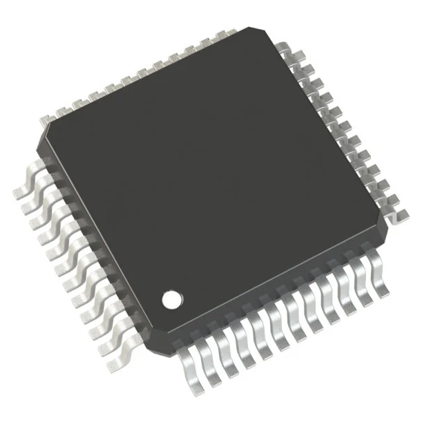
A Comprehensive Guide To MC56F8006VLF Microcontroller IC 16-Bit 32MHz 16KB (8K x 16) FLASH 48-LQFP (7x7)
- Manufacturer: NXP USA Inc.
- Product NO: MC56F8006VLF
- Package: 48-LQFP
- Datasheet:
 PDF
PDF - Stock: 28
- Sample Price: $9.01
- Bulk purchase price:
- Description: 56800E 56F8xxx Microcontroller IC 16-Bit 32MHz 16KB (8K x 16) FLASH 48-LQFP (7x7)MC56F8006/MC56F8002 Digital Signal Con Notice:
Unconfirmed payment orders may not be able to deliver the normal cancellation of the order, please communicate with the email to confirm before making the relevant payment ~ Attached email phone number The platform has the right to cancel the unconfirmed payment orders do not need to bear the responsibility of default.
Payment and disbursement


| Parameters |
|---|
56800E 56F8xxx Microcontroller IC 16-Bit 32MHz 16KB (8K x 16) FLASH 48-LQFP (7x7)
MC56F8006/MC56F8002 Digital Signal Controller
This document applies to parts marked with 2M53M.
The 56F8006/56F8002 is a member of the 56800E core-based family of digital signal controllers (DSCs). It combines, on a
single chip, the processing power of a DSP and the functionality of a microcontroller with a flexible set of
peripherals to create a cost-effective solution. Because of its low cost, configuration flexibility, and compact program
code, the 56F8006/56F8002 is well-suited for many applications. It includes many peripherals that are especially
useful for cost-sensitive applications, including:
• Industrial control
• Home appliances
• Smart sensors
• Fire and security systems
• Switched-mode power supply and power management
• Power metering
• Motor control (ACIM, BLDC, PMSM, SR, and stepper)
• Handheld power tools
• Arc detection
• Medical device/equipment
• Instrumentation
• Lighting ballast
The 56800E core is based on a dual Harvard-style architecture consisting of three execution units operating in parallel, allowing
as many as six operations per instruction cycle. The MCU-style programming model and optimized instruction set allow
straightforward generation of efficient, compact DSP and control code. The instruction set is also highly efficient for C compilers
to enable rapid development of optimized control applications.
The 56F8006/56F8002 supports program execution from internal memories. Two data operands can be accessed from the on-chip
data RAM per instruction cycle. The 56F8006/56F8002 also offers up to 40 general-purpose input/output (GPIO) lines,
depending on peripheral configuration.
The 56F8006/56F8002 digital signal controller includes up to 16 KB of program flash and 2 KB of unified data/program
RAM. Program flash memory can be independently bulk erased or erased in small pages of 512 bytes (256 words).
On-chip features include:
• Up to 32 MIPS at 32 MHz core frequency
• DSP and MCU functionality in a unified, C-efficient architecture
• On-chip memory
– 56F8006: 16 KB (8K x 16) flash memory
– 56F8002: 12 KB (6K x 16) flash memory
– 2 KB (1K x 16) unified data/program RAM
• One 6-channel PWM module
• Two 28-channel, 12-bit analog-to-digital converters (ADCs)
• Two programmable gain amplifiers (PGA) with gain up to 32x
• Three analog comparators
• One programmable interval timer (PIT)
• One high-speed serial communication interface (SCI) with
LIN slave functionality
• One serial peripheral interface (SPI)
• One 16-bit dual timer (2 x 16 bit timers)
• One programmable delay block (PDB)
• One SMBus compatible inter-integrated circuit (I2C) port
• One real time counter (RTC)
• Computer operating properly (COP)/watchdog
• Two on-chip relaxation oscillators — 1 kHz and 8 MHz (400 kHz at standby mode)
• Crystal oscillator
• Integrated power-on reset (POR) and low-voltage interrupt (LVI) module
• JTAG/enhanced on-chip emulation (OnCE™) for unobtrusive, real-time debugging
• Up to 40 GPIO lines
• 28-pin SOIC, 32-pin LQFP, 32-pin PSDIP, and 48-pin LQFP packages
56F8006/56F8002 Features
1 Core
• Efficient 16-bit 56800E family digital signal controller (DSC) engine with dual Harvard architecture
• As many as 32 million instructions per second (MIPS) at 32 MHz core frequency
• 155 basic instructions in conjunction with up to 20 address modes
• Single-cycle 16 16-bit parallel multiplier-accumulator (MAC)
• Four 36-bit accumulators, including extension bits
• 32-bit arithmetic and logic multi-bit shifter
• Parallel instruction set with unique DSP addressing modes
• Hardware DO and REP loops
• Three internal address buses
• Four internal data buses
• Instruction set supports DSP and controller functions
• Controller-style addressing modes and instructions for compact code
• Efficient C compiler and local variable support
• Software subroutine and interrupt stack with depth limited only by memory
• JTAG/enhanced on-chip emulation (EOnCE) for unobtrusive, processor speed–independent, real-time debugging
2 Operation Range
• 1.8 V to 3.6 V operation (power supplies and I/O)
• From power-on-reset: approximately 1.9 V to 3.6 V
• Ambient temperature operating range:
— –40 °C to 125 °C
3 Memory
• Dual Harvard architecture permits as many as three simultaneous accesses to program and data memory
• Flash security and protection that prevent unauthorized users from gaining access to the internal flash
• On-chip memory
— 16 KB of program flash for 56F8006 and 12 KB of program flash for 56F8002
— 2 KB of unified data/program RAM
• EEPROM emulation capability using flash
4 Interrupt Controller
• Five interrupt priority levels
— Three user programmable priority levels for each interrupt source: Level 0, 1, 2
— Unmaskable level 3 interrupts include: illegal instruction, hardware stack overflow, misaligned data access, SWI3
instruction. Maskable level 3 interrupts include: EOnCE step counter, EOnCE breakpoint unit, EOnCE trace
buffer
— Lowest-priority software interrupt: level LP
• Allow nested interrupt that higher priority level interrupt request can interrupt lower priority interrupt subroutine
• The masking of interrupt priority level is managed by the 56800E core
• One programmable fast interrupt that can be assigned to any interrupt source
• Notification to system integration module (SIM) to restart clock out of wait and stop states
• Ability to relocate interrupt vector table
5 Peripheral Highlights
• One multi-function, six-output pulse width modulator (PWM) module
— Up to 96 MHz PWM operating clock
— 15 bits of resolution
— Center-aligned and edge-aligned PWM signal mode
— Phase shifting PWM pulse generation
— Four programmable fault inputs with programmable digital filter
— Double-buffered PWM registers
— Separate deadtime insertions for rising and falling edges
— Separate top and bottom pulse-width correction by means of software
— Asymmetric PWM output within both Center Aligned and Edge Aligned operation
— Separate top and bottom polarity control
— Each complementary PWM signal pair allows selection of a PWM supply source from:
– PWM generator
– Internal timers
– Analog comparator outputs
• Two independent 12-bit analog-to-digital converters (ADCs)
— 2 x 14 channel external inputs plus seven internal inputs
— Support simultaneous and software triggering conversions
— ADC conversions can be synchronized by PWM and PDB modules
— Sampling rate up to 400 KSPS for 10- or 12-bit conversion result; 470 KSPS for 8-bit conversion result
— Two 16-word result registers
• Two programmable gain amplifier (PGAs)
— Each PGA is designed to amplify and convert differential signals to a single-ended value fed to one of the ADC
inputs
— 1X, 2X, 4X, 8X, 16X, or 32X gain
— Software and hardware triggers are available
— Integrated sample/hold circuit
— Includes additional calibration features:
– Offset calibration eliminates any errors in the internal reference used to generate the VDDA/2 output center
point
– Gain calibration can be used to verify the gain of the overall datapath
– Both features require software correction of the ADC result
• Three analog comparators (CMPs)
— Selectable input source includes external pins, internal DACs
— Programmable output polarity
— Output can drive timer input, PWM fault input, PWM source, external pin output, and trigger ADCs
— Output falling and rising edge detection able to generate interrupts
• One dual channel 16-bit multi-purpose timer module (TMR)
— Two independent 16-bit counter/timers with cascading capability
— Up to 96 MHz operating clock
— Each timer has capture and compare and quadrature decoder capability
— Up to 12 operating modes
— Four external inputs and two external outputs
• One serial communication interface (SCI) with LIN slave functionality
— Up to 96 MHz operating clock
— Full-duplex or single-wire operation
— Programmable 8- or 9- bit data format
— Two receiver wakeup methods:
– Idle line
– Address mark
— 1/16 bit-time noise detection
• One serial peripheral interface (SPI)
— Full-duplex operation
— Master and slave modes
— Programmable length transactions (2 to 16 bits)
— Programmable transmit and receive shift order (MSB as first or last bit transmitted)
— Maximum slave module frequency = module clock frequency/2
• One inter-integrated Circuit (I2C) port
— Operates up to 400 kbps
— Supports master and slave operation
— Supports 10-bit address mode and broadcasting mode
— Supports SMBus, Version 2
• One 16-bit programmable interval timer (PIT)
— 16 bit counter with programmable counter modulo
— Interrupt capability
• One 16-bit programmable delay block (PDB)
— 16 bit counter with programmable counter modulo and delay time
— Counter is initiated by positive transition of internal or external trigger pulse
— Supports two independently controlled delay pulses used to synchronize PGA and ADC conversions with input
trigger event
— Two PDB outputs can be ORed together to schedule two conversions from one input trigger event
— PDB outputs can be can be used to schedule precise edge placement for a pulsed output that generates the control
signal for the CMP windowing comparison
— Supports continuous or single shot mode
— Bypass mode supported
• Computer operating properly (COP)/watchdog timer capable of selecting different clock sources
— Programmable prescaler and timeout period
— Programmable wait, stop, and partial powerdown mode operation
— Causes loss of reference reset 128 cycles after loss of reference clock to the PLL is detected
— Choice of clock sources from four sources in support of EN60730 and IEC61508:
– On-chip relaxation oscillator
– External crystal oscillator/external clock source
– System clock (IPBus up to 32 MHz)
– On-chip low power 1 kHz oscillator
• Real-timer counter (RTC)
— 8-bit up-counter
— Three software selectable clock sources
– External crystal oscillator/external clock source
– On-chip low-power 1 kHz oscillator
– System bus (IPBus up to 32 MHz)
— Can signal the device to exit power down mode
• Phase lock loop (PLL) provides a high-speed clock to the core and peripherals
— Provides 3x system clock to PWM and dual timer and SCI
— Loss of lock interrupt
— Loss of reference clock interrupt
• Clock sources
— On-chip relaxation oscillator with two user selectable frequencies: 400 kHz for low speed mode, 8 MHz for
normal operation
— On-chip low-power 1 kHz oscillator can be selected as clock source to the RTC and/or COP
— External clock: crystal oscillator, ceramic resonator, and external clock source
• Power management controller (PMC)
— On-chip regulator for digital and analog circuitry to lower cost and reduce noise
— Integrated power-on reset (POR)
— Low-voltage interrupt with a user selectable trip voltage of 1.81 V or 2.31 V
— User selectable brown-out reset
— Run, wait, and stop modes
— Low-power run, wait, and stop modes
— Partial power down mode
• Up to 40 general-purpose I/O (GPIO) pins
— Individual control for each pin to be in peripheral or GPIO mode
— Individual input/output direction control for each pin in GPIO mode
— Hysteresis and configurable pullup device on all input pins
— Configurable slew rate and drive strength and optional input low pass filters on all output pins
— 20 mA sink/source current
• JTAG/EOnCE debug programming interface for real-time debugging
— IEEE 1149.1 Joint Test Action Group (JTAG) interface
— EOnCE interface for real-time debugging
6 Power Saving Features
• Three low power modes
— Low-speed run, wait, and stop modes: 200 kHz IP bus clock provided by ROSC
— Low-power run, wait, and stop modes: clock provided by external 32–38.4 kHz crystal
— Partial power down mode
• Low power external oscillator can be used in any low-power mode to provide accurate clock to active peripherals
• Low power real time counter for use in run, wait, and stop modes with internal and external clock sources
• 32 s typical wakeup time from partial power down modes
• Each peripheral can be individually disabled to save power
NXP Electronics components unboxing,humidity card changed color chip can used?
Hot Sales
S9KEAZ128AMLH
ARM® Cortex®-M0+ Kinetis KEA Microcontroller IC 32-Bit Single-Core 48MHz 128KB (128K x 8) FLASH 64-L..
ADG1433YRUZ
IC SWITCH SPDTX3 4.7OHM 16TSSOPElectronic components ADG1433YRUZ UNBOXING,Operational Amplifier, www..
ADG408BRUZ
ADG408BRUZ Multiplexer Switch IC, Unboxing of the electronic components. | ICONCIHP Website For more..
SP3072EEN-L/TR
Unboxing of the electronic components SP3072EEN-LTRFor more product unboxing videos, please click on..
Pricing And ODER
Stock:
0
Price:
$9.01
Quantity:
Shipping Cost
$28.63
PostNL International Mail 11-33
?Unconfirmed payment orders may not be able to deliver the normal cancellation of the order, please communicate with the email to confirm before making the relevant payment ~ Attached email phone number The platform has the right to cancel the unconfirmed payment orders do not need to bear the responsibility of default.
Shipment Date
2026/06/17 PM
Delivery Date
5-10 business days
About Logistics:
?Shipping time will be determined according to the logistics time, there will be differences in the place please understand!
| Sub-Total | $9.01 |
| Shipping: | $28.63 |
| Total | $37.64 |
Please send RFQ , we will respond immediately.
Product:
-
 Afghanistan
-
Afghanistan
-
 Albania
-
 Algeria
-
 American Samoa
-
 Andorra
-
 Angola
-
 Anguilla
-
 Antigua & Barbuda
-
 Argentina
-
 Arizona
-
 Armenia
-
 Aruba
Aruba
-
 Australia
-
 Austria
-
 Azerbaijan
-
 Bahamas
-
 Bahrain
-
 Bangladesh
-
 Barbados
-
 Belarus
-
 Belgium
-
 Belize
-
 Benin
Benin
-
 Bermuda
-
 Bhutan
-
 Bolivia
-
 Bonaire
-
 Bosnia and Herzegovina
-
 Botswana
-
 Brazil
-
 British Virgin Islands
-
 Brunei
-
 Bulgaria
-
 Burkina Faso
-
 Burundi
-
 California
-
 Cambodia
-
 Cameroon
-
 Canada
-
 Cape Verde
-
 Cayman Islands
-
 Central African Republic
-
 Chad
Chad
-
 Chile
Chile
-
 Colombia
-
 Colorado
-
 Congo
Congo
-
 Cook Islands
-
 Costa Rica
-
 Côte d'Ivoire
-
 Croatia
-
 Curaçao
-
 Curacao
-
 Cyprus
-
 Czech Republic
-
 Democratic Republic of Congo
-
Democratic Republic of the Congo
-
 Denmark
-
 Djibouti
-
 Dominica
-
 Dominican Republic
-
 East Timor
-
 Ecuador
-
 Egypt
Egypt
-
 El Salvador
-
 Eritrea
-
 Estonia
-
Eswatini
-
 Ethiopia
-
 Faroe Islands
-
 Fiji
Fiji
-
 Finland
-
 France
-
 French Guiana
-
 French Polynesia
-
 Gabon
Gabon
-
 Gambia
-
 Georgia
-
 Germany
-
 Ghana
Ghana
-
 Gibraltar
-
 Greece
-
 Greenland
-
 Grenada
-
 Guadeloupe
-
 Guam
Guam
-
 Guatemala
-
 Guinea
-
 Guyana
-
 Haiti
Haiti
-
 Honduras
-
 Hong Kong
-
Hong Kong, China
-
 Hungary
-
 Iceland
-
 Idaho
Idaho
-
 India
India
-
 Indonesia
-
 Iraq
Iraq
-
 Ireland
-
 Israel
-
 Italy
Italy
-
Ivory Coast
-
 Jamaica
-
 Japan
Japan
-
 Jordan
-
 Kazakhstan
-
 Kenya
Kenya
-
 Kuwait
-
 Kyrgyzstan
-
 Laos
Laos
-
 Latvia
-
 Lebanon
-
 Lesotho
-
 Liberia
-
 Libya
Libya
-
 Liechtenstein
-
Liechtenstein (Switzerland)
-
 Lithuania
-
 Luxembourg
-
Macao, China
-
 Macau
Macau
-
 Macedonia
-
 Madagascar
-
 Malawi
-
 Malaysia
-
 Maldives
-
 Mali
Mali
-
 Malta
Malta
-
 Marshall Islands
-
 Martinique
-
 Mauritania
-
 Mauritius
-
 Mexico
-
 Micronesia
-
 Moldova
-
 Monaco
-
Monaco (France)
-
 Mongolia
-
 Montenegro
-
 Montserrat
-
 Morocco
-
 Mozambique
-
 Myanmar
-
 Namibia
-
 Nepal
Nepal
-
 Netherlands
-
 Netherlands Antilles
-
 Nevada
-
 New Caledonia
-
 New Zealand
-
 Nicaragua
-
 Niger
Niger
-
 Nigeria
-
North Macedonia
-
 Northern Mariana Islands
-
 Norway
-
 Oman
Oman
-
 Oregon
-
 Other States in US
-
 Pakistan
-
 Palau
Palau
-
Palestinian Authority
-
 Palestinian Territories
-
 Panama
-
 Papua New Guinea
-
 Paraguay
-
 Peru
Peru
-
 Philippines
-
 Poland
-
 Portugal
-
 Puerto Rico
-
 Qatar
Qatar
-
Republic of Moldova
-
Rest of the United States
-
 Réunion
-
Reunion
-
 Romania
-
Rota (Northern Mariana Islands)
-
 Russian
-
Russian Federation
-
 Rwanda
-
Saint Kitts and Nevis
-
 Saint Lucia
-
Saint Maarten (Dutch part)
-
 Saint Martin (French part)
-
 Saint Vincent and the Grenadines
-
Saipan (Northern Mariana Islands)
-
 Samoa
Samoa
-
 San Marino
-
 Saudi Arabia
-
 Senegal
-
 Serbia
-
 Seychelles
-
 Sierra Leone
-
 Singapore
-
 Slovakia
-
 Slovenia
-
Solomon Islands
-
 South Africa
-
 South Korea
-
 Spain
Spain
-
 Sri Lanka
-
 St. Kitts and Nevis
-
 St. Maarten
-
 Suriname
-
 Swaziland (Eswatini)
-
 Sweden
-
 Switzerland
-
 Syria
Syria
-
 Taiwan
-
Taiwan, China
-
 Tajikistan
-
 Tanzania
-
 Thailand
-
Tinian (Northern Mariana Islands)
-
 Togo
Togo
-
 Tonga
Tonga
-
 Trinidad and Tobago
-
 Tunisia
-
 Turkey
-
 Turks and Caicos Islands
-
 Uganda
-
 Ukraine
-
 United Arab Emirates
-
 United Kingdom
-
United Kingdom (Great Britain)
-
 United States
-
 United States Virgin Islands
-
 Uruguay
-
 Utah
Utah
-
 Uzbekistan
-
 Vanuatu
-
 Venezuela
-
 Vietnam
-
 Wallis and Futuna
-
 Washington
-
 Yemen
Yemen
-
 Zambia
-
 Zimbabwe
| Shipping method | Costs | Delivery Time | |
|---|---|---|---|
 SF Express SF Express |
$21.08 | 6-8 business days |


