FIRST ORDER
FREE 10% DISCOUNT




NXP USA Inc.
Alarms, Buzzers, and Sirens
-
Stacked
Scrolling
|
Img
|
Pdf
|
Part Number
|
Manufacturers
|
Desc
|
In Stock
|
Packing
|
Rfq
|
||||||||||||||||||||||||||||||||
|---|---|---|---|---|---|---|---|---|---|---|---|---|---|---|---|---|---|---|---|---|---|---|---|---|---|---|---|---|---|---|---|---|---|---|---|---|---|---|---|
|
|

|
USB Controller USB 2.0, USB 3.0 USB Interface 16-HVSON (3.5x5.5)
|
67
|
16-VDFN Exposed Pad
|
|
||||||||||||||||||||||||||||||||||
|
|
|
Diode Array
|
9621
|
|
|||||||||||||||||||||||||||||||||||
|
|
|
IC
|
7287
|
|
|||||||||||||||||||||||||||||||||||
|
|
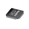
CPU12 HC12 Microcontroller IC 16-Bit 8MHz 32KB (32K x 8) FLASH 80-QFP (14x14) Introduction The MC68HC912B32, MC68HC12BE32 and MC68HC(9)12BC32, are 16-bit microcontroller units (MCUs) composed of standard on-chip peripherals. The multiplexed external bus can also operate in an 8-bit narrow mode for interfacing with single 8-bit wide memory in lower-cost systems. Features Features include: • 16-bit CPU12: – Upwardly compatible with the M68HC11 instruction set – Interrupt stacking and programmer’s model identical to the M68HC11 – 20-bit arithmetic logic unit (ALU) – Instruction queue – Enhanced indexed addressing – Fuzzy logic instructions • Multiplexed bus: – Single chip or expanded – 16-bit by 16-bit wide or 16-bit by 8-bit narrow modes • Memory: – 32-Kbyte FLASH electrically erasable, programmable read-only memory (EEPROM) with 2-Kbyte erase-protected boot block — MC68HC912B32 and MC68HC912BC32 only – 32-Kbyte ROM — MC68HC12BE32 and MC68HC12BC32 only – 768-byte EEPROM – 1-Kbyte random-access memory (RAM) with single-cycle access for aligned or misaligned read/write • 8-channel, 10-bit analog-to-digital converter (ATD) • 8-channel standard timer module (TIM) — MC68HC912B32 and MC68HC(9)12BC32 only: – Each channel fully configurable as either input capture or output compare – Simple pulse-width modulator (PWM) mode – Modulus reset of timer counter • Enhanced capture timer (ECT) — MC68HC12BE32 only: – 16-bit main counter with 7-bit prescaler – Eight programmable input capture or output compare channels; four of the eight input captures with buffer – Input capture filters and buffers, three successive captures on four channels, or two captures on four channels with a capture/compare selectable on the remaining four – Four 8-bit or two 16-bit pulse accumulators – 16-bit modulus down-counter with 4-bit prescaler – Four user-selectable delay counters for signal filtering • 16-bit pulse accumulator: – External event counting – Gated time accumulation • Pulse-width modulator (PWM): – 8-bit, 4-channel or 16-bit, 2-channel – Separate control for each pulse width and duty cycle – Programmable center-aligned or left-aligned outputs • Serial interfaces: – Asynchronous serial communications interface (SCI) – Synchronous serial peripheral interface (SPI) – J1850 byte data link communication (BDLC), MC68HC912B32 and MC68HC12BE32 only – Controller area network (CAN), MC68HC(9)12BC32 only • Computer operating properly (COP) watchdog timer, clock monitor, and periodic interrupt timer • Slow-mode clock divider • 80-pin quad flat pack (QFP) • Up to 63 general-purpose input/output (I/O) lines • Single-wire background debug mode (BDM) • On-chip hardware breakpoints NXP Electronics components unboxing,humidity card changed color chip can used? |
8945
|
80-QFP
|
|
||||||||||||||||||||||||||||||||||
|
|
|
HC05 HC05 Microcontroller IC 8-Bit 2.1MHz 15KB (15K x 8) OTP 52-PLCC (19.1x19.1)
|
9619
|
52-LCC (J-Lead)
|
|
||||||||||||||||||||||||||||||||||
|
|
|
RF Mosfet 28 V 1.2 A 1.99GHz 13dB 26W NI-880H-2L
|
3842
|
SOT-957A
|
|
||||||||||||||||||||||||||||||||||
|
|
|
Charger IC Lithium Ion/Polymer 8-UDFN (3x2)
|
9481
|
8-UFDFN Exposed Pad
|
|
||||||||||||||||||||||||||||||||||

|
|
I/O Expander
How do you identify which pin is pin 1 of an IC integrated circuit chip? |ICONECHIPFor more product unboxing videos, please click on the link
|
3068
|
-
|
|
||||||||||||||||||||||||||||||||||
|
|
|
Bipolar Motor Driver Power MOSFET Parallel 20-TSSOP
|
2241
|
20-TSSOP (0.173", 4.40mm Width) Exposed Pad
|
|
||||||||||||||||||||||||||||||||||
|
|
|
ARM® Cortex®-M4F S32K Microcontroller IC 32-Bit Single-Core 112MHz 512KB (512K x 8) FLASH 64-LQFP (10x10)
|
8671
|
64-LQFP
|
|
||||||||||||||||||||||||||||||||||
|
|
|
NAND Gate IC 4 Channel Schmitt Trigger 14-SSOP
|
6
|
14-SSOP (0.209", 5.30mm Width)
|
|
||||||||||||||||||||||||||||||||||
|
|
|
NAND Gate IC 1 Channel 5-TSSOP
|
5583
|
5-TSSOP, SC-70-5, SOT-353
|
|
||||||||||||||||||||||||||||||||||
|
|
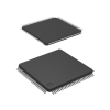
HCS12 HCS12 Microcontroller IC 16-Bit 25MHz 128KB (128K x 8) FLASH 112-LQFP (20x20) Overview The MC9S12DT128 microcontroller unit (MCU) is a 16-bit device composed of standard on-chip peripherals including a 16-bit central processing unit (HCS12 CPU), 128K bytes of Flash EEPROM, 8K bytes of RAM, 2K bytes of EEPROM, two asynchronous serial communications interfaces (SCI), two serial peripheral interfaces (SPI), an 8-channel IC/OC enhanced capture timer, two 8-channel, 10-bit analog-to-digital converters (ADC), an 8-channel pulse-width modulator (PWM), a digital Byte Data Link Controller (BDLC), 29 discrete digital I/O channels (Port A, Port B, Port K and Port E), 20 discrete digital I/O lines with interrupt and wakeup capability, three CAN 2.0 A, B software compatible modules (MSCAN12), a Byteflight module and an Inter-IC Bus. The MC9S12DT128 has full 16-bit data paths throughout. However, the external bus can operate in an 8-bit narrow mode so single 8-bit wide memory can be interfaced for lower cost systems. The inclusion of a PLL circuit allows power consumption and performance to be adjusted to suit operational requirements. Features • HCS12 Core – 16-bit HCS12 CPU i. Upward compatible with M68HC11 instruction set ii. Interrupt stacking and programmer’s model identical to M68HC11 iii.20-bit ALU iv. Instruction queue v. Enhanced indexed addressing – MEBI (Multiplexed External Bus Interface) – MMC (Module Mapping Control) – INT (Interrupt control) – BKP (Breakpoints) – BDM (Background Debug Module) • CRG (Clock and Reset Generator) – Choice of low current Colpitts oscillator or standard Pierce Oscillator – PLL – COP watchdog – real time interrupt – clock monitor • 8-bit and 4-bit ports with interrupt functionality – Digital filtering – Programmable rising or falling edge trigger • Memory – 128K Flash EEPROM – 2K byte EEPROM – 8K byte RAM • Two 8-channel Analog-to-Digital Converters – 10-bit resolution – External conversion trigger capability • Three 1M bit per second, CAN 2.0 A, B software compatible modules – Five receive and three transmit buffers – Flexible identifier filter programmable as 2 x 32 bit, 4 x 16 bit or 8 x 8 bit – Four separate interrupt channels for Rx, Tx, error and wake-up – Low-pass filter wake-up function – Loop-back for self test operation • Enhanced Capture Timer – 16-bit main counter with 7-bit prescaler – 8 programmable input capture or output compare channels – Four 8-bit or two 16-bit pulse accumulators • 8 PWM channels – Programmable period and duty cycle – 8-bit 8-channel or 16-bit 4-channel – Separate control for each pulse width and duty cycle – Center-aligned or left-aligned outputs – Programmable clock select logic with a wide range of frequencies – Fast emergency shutdown input – Usable as interrupt inputs • Serial interfaces – Two asynchronous Serial Communications Interfaces (SCI) – Two Synchronous Serial Peripheral Interface (SPI) – Byteflight • Byte Data Link Controller (BDLC) • SAE J1850 Class B Data Communications Network Interface – Compatible and ISO Compatible for Low-Speed (<125 Kbps) Serial Data Communications in Automotive Applications • Inter-IC Bus (IIC) – Compatible with I2C Bus standard – Multi-master operation – Software programmable for one of 256 different serial clock frequencies • 112-Pin LQFP and 80-Pin QFP package options – I/O lines with 5V input and drive capability – 5V A/D converter inputs – Operation at 50MHz equivalent to 25MHz Bus Speed – Development support – Single-wire background debug™ mode – On-chip hardware breakpoints NXP Electronics components unboxing,humidity card changed color chip can used? |
7608
|
112-LQFP
|
|
||||||||||||||||||||||||||||||||||
|
|
|
HC08 HC08 Microcontroller IC 8-Bit 8MHz 1.5KB (1.5K x 8) FLASH 20-SOIC
|
8357
|
20-SOIC (0.295", 7.50mm Width)
|
|
||||||||||||||||||||||||||||||||||
|
|
|
RF Mosfet 28 V 1.05 A 2.16GHz ~ 2.17GHz 13.5dB 23W NI-780H-2L
|
3283
|
SOT-957A
|
|
||||||||||||||||||||||||||||||||||
|
|
|
System Basis Chip PMIC 32-LQFP (7x7)
|
9417
|
32-LQFP
|
|
||||||||||||||||||||||||||||||||||
|
|
|
Real Time Clock (RTC) IC
|
4586
|
|
|||||||||||||||||||||||||||||||||||
|
|
|
e200z2, e200z4, e200z4 MPC57xx Microcontroller IC 32-Bit Tri-Core 80MHz/160MHz 6MB (6M x 8) FLASH 256-MAPPBGA (17x17)
|
6267
|
256-LBGA
|
|
||||||||||||||||||||||||||||||||||
|
|
|
ARM® Cortex®-A72 Microprocessor IC QorIQ® Layerscape 4 Core, 64-Bit 1.8GHz 1292-FCPBGA (37.5x37.5)
|
7829
|
1292-BFBGA, FCBGA
|
|
||||||||||||||||||||||||||||||||||
|
|
|
Zener Diode 9.1 V 300 mW ±5% Surface Mount SOD-523
|
9507
|
SC-79, SOD-523
|
|
||||||||||||||||||||||||||||||||||
|
|
|
ARM® Cortex®-M0 LPC11Axx Microcontroller IC 32-Bit Single-Core 50MHz 8KB (8K x 8) FLASH 32-HVQFN (7x7)
How do you identify which pin is pin 1 of an IC integrated circuit chip? |ICONECHIPFor more product unboxing videos, please click on the link
|
9606
|
32-VQFN Exposed Pad
|
|
||||||||||||||||||||||||||||||||||
-100x100.png "A Comprehensive Guide To MC56F8322VFAE Microcontroller IC 16-Bit 60MHz 32KB (16K x 16) FLASH 48-LQFP (7x7)")
|
|
56800E 56F8xxx Microcontroller IC 16-Bit 60MHz 32KB (16K x 16) FLASH 48-LQFP (7x7) Device Description The 56F8322 and 56F8122 are members of the 56800E core-based family of controllers. Each combines, on a single chip, the processing power of a Digital Signal Processor (DSP) and the functionality of a microcontroller with a flexible set of peripherals to create an extremely cost-effective solution. Because of their low cost, configuration flexibility, and compact program code, the 56F8322 and 56F8122 are well-suited for many applications. These devices include many peripherals that are especially useful for automotive control (56F8322 only); industrial control and networking; motion control; home appliances; general purpose inverters; smart sensors; fire and security systems; power management; and medical monitoring applications. The 56800E core is based on a Harvard-style architecture consisting of three execution units operating in parallel, allowing as many as six operations per instruction cycle. The MCU-style programming model and optimized instruction set allow straightforward generation of efficient, compact DSP and control code. The instruction set is also highly efficient for C Compilers to enable rapid development of optimized control applications. The 56F8322 and 56F8122 support program execution from internal memories. Two data operands can be accessed from the on-chip data RAM per instruction cycle. These devices also provide one external dedicated interrupt line and up to 21 General Purpose Input/Output (GPIO) lines, depending on peripheral configuration. 56F8322 Features The 56F8322 controller includes 32KB of Program Flash and 8KB of Data Flash, each programmable through the JTAG port, and 4KB of Program RAM and 8KB of Data RAM. A total of 8KB of Boot Flash is incorporated for easy customer inclusion of field-programmable software routines that can be used to program the main Program and Data Flash memory areas. Both Program and Data Flash memories can be independently bulk erased or erased in pages. Program Flash page erase size is 1KB. Boot and Data Flash page erase size is 512 bytes. The Boot Flash memory can also be either bulk or page erased. A key application-specific feature of the 56F8322 is the inclusion of one Pulse Width Modulator (PWM) module. This module incorporates three complementary, individually programmable PWM signal output pairs and is also capable of supporting six independent PWM functions to enhance motor control functionality. Complementary operation permits programmable dead time insertion, distortion correction via current sensing by software, and separate top and bottom output polarity control. The up-counter value is programmable to support a continuously variable PWM frequency. Edge-aligned and center-aligned synchronous pulse width control (0% to 100% modulation) is supported. The device is capable of controlling most motor types: ACIM (AC Induction Motors); both BDC and BLDC (Brush and Brushless DC motors); SRM and VRM (Switched and Variable Reluctance Motors); and stepper motors. The PWM incorporates fault protection and cycle-by-cycle current limiting with sufficient output drive capability to directly drive standard optoisolators. A “smoke-inhibit”, write-once protection feature for key parameters is also included. A patented PWM waveform distortion correction circuit is also provided. Each PWM is double-buffered and includes interrupt controls to permit integral reload rates to be programmable from 1/2 (center-aligned mode only) to 16. The PWM module provides reference outputs to synchronize the Analog-to-Digital Converters (ADCs) through Quad Timer C, channel 2. The 56F8322 incorporates one Quadrature Decoder capable of capturing all four transitions on the two-phase inputs, permitting generation of a number proportional to actual position. Speed computation capabilities accommodate both fast- and slow-moving shafts. An integrated watchdog timer in the Quadrature Decoder can be programmed with a time-out value to alarm when no shaft motion is detected. Each input is filtered to ensure only true transitions are recorded. This controller also provides a full set of standard programmable peripherals that include two Serial Communications Interfaces (SCIs), two Serial Peripheral Interfaces (SPIs), two Quad Timers and FlexCAN. Any of these interfaces can be used as General Purpose Input/Outputs (GPIOs) if that function is not required. A Flex Controller Area Network interface (CAN Version 2.0 B-compliant) and an internal interrupt controller are also a part of the 56F8322. NXP Electronics components unboxing,humidity card changed color chip can used? |
8578
|
48-LQFP
|
|
||||||||||||||||||||||||||||||||||
|
|
|
Coldfire V2 SCF52xx Microcontroller IC 32-Bit Single-Core 120MHz ROMless 144-LQFP (20x20)
|
6347
|
144-LQFP
|
|
||||||||||||||||||||||||||||||||||
|
|
|
RF Mosfet 26 V 600 mA 880MHz 17.8dB 14W TO-270-2
|
6450
|
TO-270-2
|
|
||||||||||||||||||||||||||||||||||
|
|
|
HC11 HC11 Microcontroller IC 8-Bit 3MHz ROMless 44-QFP (10x10)
|
6879
|
44-QFP
|
|
||||||||||||||||||||||||||||||||||
|
|
|
MOSFET N-CH SOT-23
|
7913
|
|
|||||||||||||||||||||||||||||||||||
|
|
|
System Basis Chip Interface 20-HVSON (3.5x5.5)
|
8698
|
20-VFDFN Exposed Pad
|
|
||||||||||||||||||||||||||||||||||
|
|
|
ARM® Cortex®-A72 Microprocessor IC QorIQ® Layerscape 8 Core, 64-Bit 1.8GHz 1292-FCPBGA (37.5x37.5)
|
6534
|
1292-BFBGA, FCBGA
|
|
||||||||||||||||||||||||||||||||||
|
|
|
Zener Diode 39 V 300 mW ±2% Surface Mount SOD-523
|
7618
|
SC-79, SOD-523
|
|
||||||||||||||||||||||||||||||||||
|
|
|
ARM1136JF-S Microprocessor IC i.MX35 1 Core, 32-Bit 400MHz 400-MAPBGA (17x17)
|
90
|
400-LFBGA
|
|
||||||||||||||||||||||||||||||||||